Contents
What is a Snubber Circuit?
General Classifications of Snubber
Commonly Used Snubbers in Practical Applications
Snubber Circuit Design
Methodology of Snubber Circuit Analysis
Summary
What is a Snubber Circuit?

A trial snubber circuit
Damping voltage to reduce EMI
Minimizing total switching losses
Limiting dV/dt or dl/DT
Minimizing or eliminating a current or voltage spike, or both
Shaping the load line to maintain it in the safe operating area
Moving power dissipation from the switch to useful load or resistor
A Transient Voltage Suppressor
General Classifications of Snubber
Lossy or Dissipative
Non-lossy or Non-dissipative
Lossy and Non-lossy Snubber Power Loss Comparison
Commonly Used Snubbers in Practical Applications
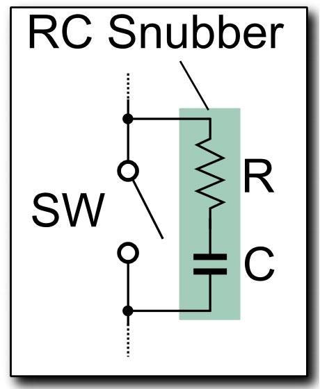
RC Snubber
Some RC Snubber Circuits
Buck Converter

A buck converter circuit diagram
DCDC Synchronous Rectifier

A DCDC synchronous rectifier circuit diagram, Note the two snubber circuits.
Boost Converter Topology

A circuit diagram for a boost converter topology, Note the two snubber circuits.
RCD Snubber
Some RCD Snubber Circuits
Flyback Converter
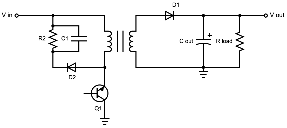
A flyback converter circuit diagram
Forward Converter

A forward converter circuit diagram. Note the snubber circuit.
Snubber Diode
Snubber Circuit Design

A snubber circuit design diagram
The stored energy in the snubber capacitor must be higher than the inductance energy in the circuit
The time constant of the snubber circuit should be 10% of the expected on time
Methodology of Snubber Circuit Analysis
Quantizing the Transient
Frequency Response
RC Snubber Model
